IC 7473, 7474, 7475, 7476 Pinout Diagram and Data Sheet
IC 7473 PinOut Diagram
Here, you can see the pin diagram of IC 7473.
The IC 7473 or mostly known as 74LS73 is a dual JK flip-flop logic gate IC. It is a negative edge-triggered IC. It has two independent JK Flip Flops. They have complementary outputs. These Flip Flops are negative edge triggered. It is also referred to as a JK Master Slave Flip Flop. During the positive transition of the clock input, the data got transferred from the J and K input to the master while during the negative transition, the data is transferred from the master to slave. So you may understand the data is first transferred from the J and K input to the master then it is transferred to the slave.
Now, let's see the features of the IC 7473
1. It has two J-K Master-Slave Flip Flop
2. It supports wide operating conditions and a large operating voltage range.
3. The output of the IC 7473 is directly CMOS, NMOS, and TTL Logic.
The IC 74LS73 can be operated from 0 degrees to 70 degrees centigrade temperature. And when the voltage at its output terminal reaches 2V, it will be considered as output HIGH, and when the voltage decreases to 0.8V then it will be considered as output LOW.
IC 7474 Pinout Diagram
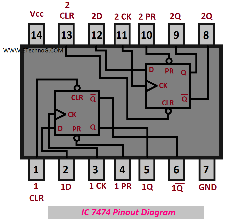
Here, you can see the pin diagram of IC 7474
IC 7474 or mostly known as IC 74LS74 is a dual D Flip Flop positive edge-triggered IC. It has two independent D Flip Flops with complementary outputs. It has a D input and a Q output. The data in the D input may be changed during the high or low clock but it does not affect the output and the delay times also do not affect it. The IC 7474 can be operated up to 7V voltage and 0 to +70 degrees centigrade temperature. The main features of the IC 74LS74 are, that it provides very fast switching, low propagation delay, large operating mode, etc.
IC 7475 Pinout Diagram
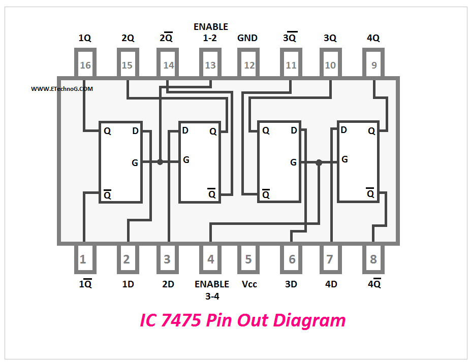
Here, you can see the pin diagram of IC7475.
The IC 7475 mostly known as 74HC75 is a 16-pin IC that contains four independent and transparent D latches. You will be seen in the pin diagram the two latches have a common enable which means the first two latches have the same enable and the second two latches have the same enable. Among the different inputs, the D and clock inputs are synchronous inputs whereas Set and Reset inputs are asynchronous inputs. The main features of the IC 7475 are, that it has 4-bit bistable latches, low operating voltage ranges, and wide operating conditions. It can be operated from 4.75 to 5.25V voltage ranges and 0 to +70 degrees centigrade temperature.
IC 7476 Pinout Diagram
Here, you can see the pin diagram of IC 7476
The IC 7476 commonly known as IC 74LS76 is a dual JK flip IC with Set and Clear Input. The Clock, Clear inputs are active low inputs. During the High-Low Clock Transition, input data is transferred to the output. It is also a 16-pin IC. The IC 7476 can be operated from 4.75 to 5.25V and 0 to +70 degrees centigrade temperature. It works with standard TTL voltage and provides a very fast switching speed.
Read Also:


