IC 74147 Pin Diagram, Internal Circuit, Truth Table
IC 74147 is a digital encoder IC that encodes 9 input lines into 4 output lines. It is also known as the Decimal to BCD priority encoder. The priority encoder term is used because it provides encoding for the highest-order data lines as a first priority. It is made up using Transistor-Transistor Logic(TTL) technology. It is a 10 to 4 encoder IC. In this article, we are going to see IC 74147 Pin Diagram, IC 74147 Internal Circuit Diagram, and IC 74147 Truth table or function table.
The general specifications of this IC are,
- It operates at 4.5V to 5.5 DC voltage.
- It delivers output current from low 70µA to high 8mA
- It operates at the temperature from -55℃ to 70℃
- Logic Case packaging type: DIP
- Mounting Type: Through Hole
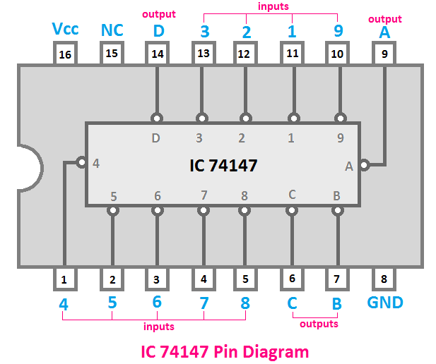
IC 74147 Pin Diagram
Here, you can see the pin diagram of IC 74147
You can see there is a total of 16 pins.
Pin No. 1 - 4 (input)
Pin No. 2 - 5 (input)
Pin No. 3 - 6 (input)
Pin No. 4 - 7 (input)
Pin No. 5 - 8 (input)
Pin No. 6 - C (output)
Pin No. 7 - B (output)
Pin No. 8 - Ground (GND)
Pin No. 9 - A (output)
Pin No. 10 - 9 (input)
Pin No. 11 - 1 (input)
Pin No. 12 - 2 (input)
Pin No. 13 - 3 (input)
Pin No. 14 - D (output)
Pin No. 15 - Not Connected (NC)
Pin No. 16 - Vcc or positive power supply
IC 74147 Internal Circuit Diagram
Here, you can see the internal circuit diagram of IC 74147
IC 74147 Truth Table/Function Table
Here, you can see the truth table of IC 74147
Read Also:


