IC 7400 Pin Diagram, Circuit design, Datasheet, Application

IC 7400
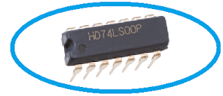
IC 7400 is a fourteen-pin Logic Gate IC. The IC 7400 consists of four NAND Gates. The NAND Gate is also called the Universal Gate. The NAND gate has a total of three terminals, two input terminals, and one output terminal. All NAND Gates are independent. IC 7400 is also called Quad 2-input NAND Gate IC.
Pin diagram of IC 7400:
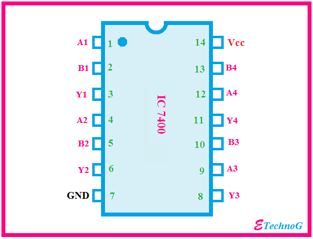
The IC 7400 has fourteen pins including Vcc and ground pins. The simple pin diagram is shown below,
Operating Condition of IC 7400:
1. The IC 7400 can operate from 4.5V DC to 5.25V DC voltage. So power supply to the IC should be given in that range.
2. It can identify a signal as a high signal if the signal has a voltage above 2V.
3. It can identify a signal as a low signal if the signal has a voltage below 0.8V
4. The Ic 7400 can withstand up to 70-degree centigrade temperature so the operating temperature should be below that temperature.
Electrical Characteristics:
1. The high-level input current is 20 micro-amperes at maximum Vcc and input voltage 2.7V
2. The low-level input current is -0.36 mA at maximum Vcc and input voltage 0.4V
3. Supply current with output HIGH is 1.6 mA at Maximum Vcc
4. Supply current with output LOW is 4.4 mA at Maximum Vcc
5. The short circuit output current is -20 to -100 mA at maximum Vcc
The Internal Structure of IC 7400:
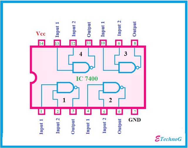
The IC 7400 has four independent NAND gates which are shown in the below figure,
Pin Description of IC 7400:
Pins | Description |
Pin 1 | It is connected to the Input(A) of NAND Gate 1 |
Pin 2 | Input(B) of NAND Gate 1 |
Pin 3 | It is connected to the Output(Y) of NAND Gate 1 |
Pin 4 | Input(A) of NAND Gate 2 |
Pin 5 | Input(B) of NAND Gate 2 |
Pin 6 | This pin provides the Output(Y) of NAND Gate 2 |
Pin 7 | Ground Pin which is used to provide the power supply to the IC. |
Pin 8 | It is connected to the Output(Y) of NAND Gate 3 |
Pin 9 | It is connected to the Input(A) of NAND Gate 3 |
Pin 10 | Input(B) of NAND Gate 3 |
Pin 11 | It is the output(Y) pin of the NAND Gate 4 |
Pin 12 | It is the input(A) pin of the NAND Gate 4 |
Pin 13 | It is the input(B) pin of the NAND Gate 4 |
Pin 14 | It is Vcc pin which used to provide the power supply to the IC. |
Application of IC 7400:
1. The NAND gate is a universal gate so it can be used to make other gates like NOT, AND gates, etc.
2. They are used in digital electronics projects.
Read Also:
Thank you for visiting the website. keep visiting for more updates.


