Microcontroller 8051 Architecture and Block Diagram Explained
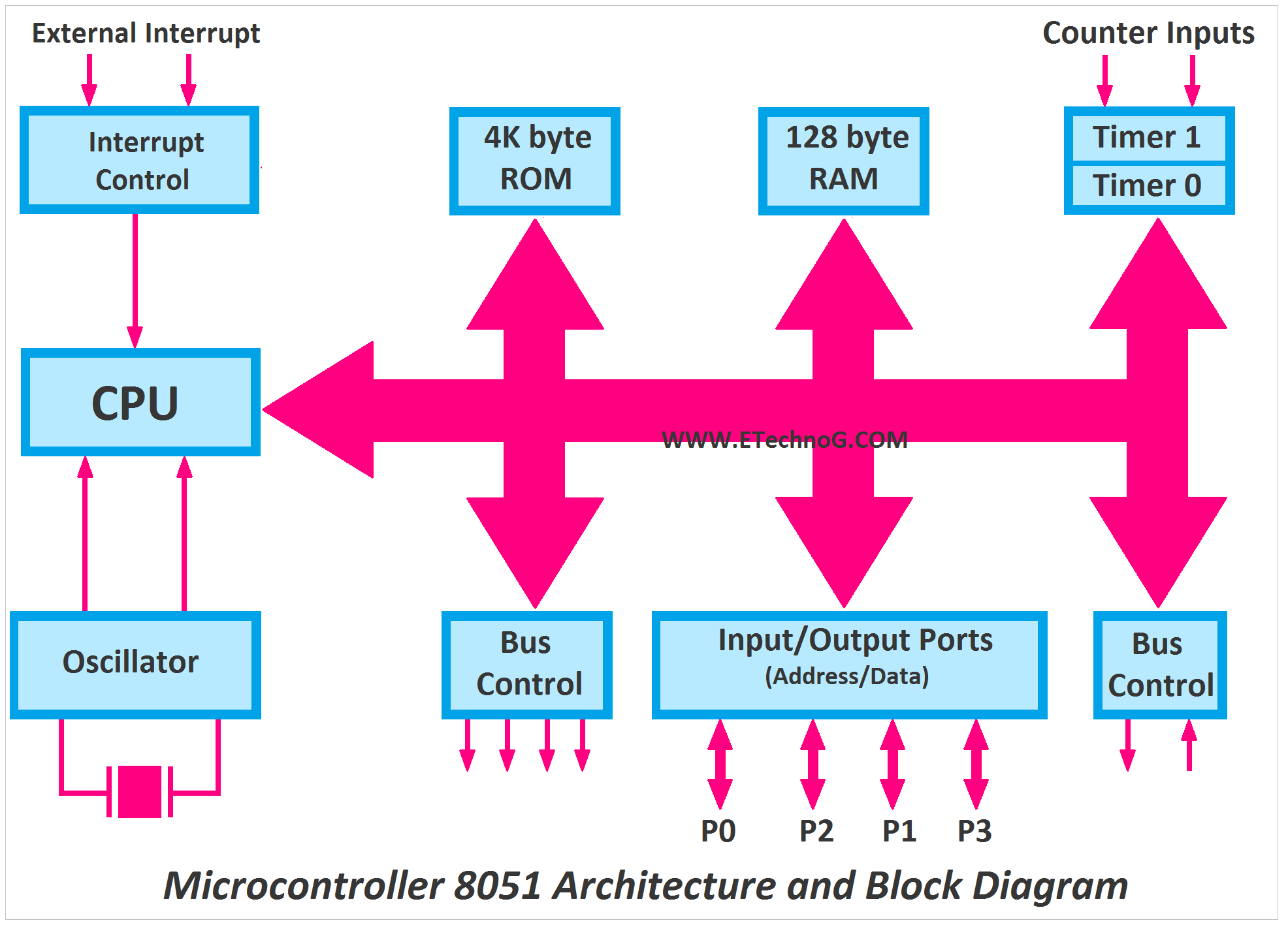
A microcontroller is more than a microprocessor. In this article, we are going to see the internal architecture of microcontroller 8051 in the form of a block diagram. It is a 40-pin DIP(Dual Inline Package), 8-bit device.
The main important blocks are explained below,
CPU(Central Processing Unit)
CPU is the main part of the microcontroller that actually does all the processing work. It is the brain of the whole circuit. The CPU has its own control circuit, Arithmetic, and logical units. It performs all the logical and mathematical operations. A user can not access the processor or CPU of the microcontroller. There are so many different circuits available between the CPU and external pins. The CPU is internally connected or interfaced with the memory units such as ROM and RAM. CPU works according to the instructions or programs stored in the ROM. At the starting of processing, it fetches the data from the ROM and performs.
Oscillator and Timers
It is an electronic pulse signal generator circuit. It provides the pulse signal to the CPU to complete its operation and to work with cycles per unit time. It is an on-chip crystal oscillator mounted outside of the CPU. The crystal frequency of this oscillator is 12 MHz. Also, the microcontroller has 2 16-bit timers.
Memory Units
The 8051 microcontroller has a 4kb ROM( Read Only Memory), and 128 byte RAM(Random Acess Memory). The 4kb ROM is used for the preloaded or stored program. The program is stored in the ROM, according to this program, the CPU works. CPU only can read or fetch data from the ROM but it can not write or store any data to the ROM. RAM is used to store data temporarily during the operation or program execution. CPU can store data in the RAM.
Interrupts
The interrupt is the subroutine call that interrupts the main ongoing program execution in the CPU and tells to execute another important task or program. For, example the CPU performs any logical operation, but the user wants to do some more important arithmetic operation immediately. Here the interrupt system helps a lot to stop the current operation of the CPU and start the new operation. Once the task is completed, the CPU again starts its own work from where it leaves. In other words, we can say the interrupts help for the emergency operations.
There are mainly five interrupt sources in the microcontroller 8051,
- TF0 - it is the Timer 0 overflow interrupt
- TF1 - it is the Timer 2 overflow interrupt
- INT0 - it is an external hardware interrupt
- INT1 - it is also an external hardware interrupt
- R1/T1 - it is the serial communication interrupt
Input/Output Ports
The 8051 microcontroller has four parallel 8-bit ports such as P0, P1, P2, and P3. These ports are bidirectional and these are used to carry both address and data.
Bus
The system bus in the microcontroller connects all the circuits or components(such as memory, timers, and ports) to the CPU. The system bus consists of an 8-bit data bus and a 16-bit address bus. The address bus helps to carry the memory addresses where the data is stored whereas the data bus helps to carry the actual data.
Read Also:

