Understand CPU Block Diagram and Architecture
CPU or Central Processing Unit is the main part of a computer system. Basically, a CPU is an electronic circuit made of different types of semiconductor devices. It performs all tasks of a computer. The main function of a CPU is to take input signals from the input devices of the computer system such as a Mouse, Keyboard, Microphone, etc, and process them. after processing the input signals CPU creates the output signals and supplies them to the output devices such as Monitor, Speaker, Printer, etc. In this article, we are going to understand the CPU Block diagram and Architecture. This will help you to understand the working principle of the CPU. The block diagram of CPU is explained in detail in the below section.
CPU Block Diagram
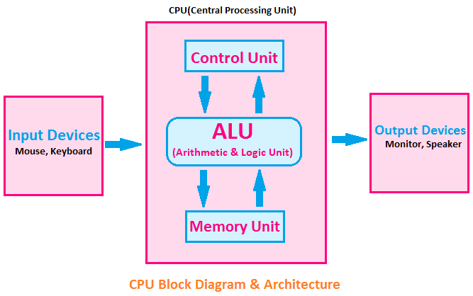
Here, you can see the block diagram of CPU below.
The above block diagram provides a visual representation of the various components and their interconnections within the CPU. And it also shows how the CPU is connected to external devices such as input devices(Mouse, Keyboards), output devices(Monitor, speakers), etc.
In the above block diagram of CPU, you can see there are mainly three blocks of the CPU - 1. Control Unit or CU 2. Arithmetic & Logic Unit or ALU 3. Memory Unit
Let's discuss the function of each block of the CPU.
Control Unit or CU
The main function of the Control Unit of a CPU is to control all components of the ALU Circuit. The components of the ALU are required to control and timing signals to perform any task. So the control unit of the CPU provides the appropriate control and timing signals to each component of the ALU. Control Unit consisting of Clock circuit, pulse generator circuit, and oscillator circuits. In simple words, the all requirements of the ALU are fulfilled by the control unit.
The control unit of the CPU monitors and controls all the tasks performed by the ALU. In fact, the control unit only decides the cycle time, priorities of tasks, etc. The control unit not only controls the performance of the ALU but also helps the ALU to communicate with other devices such as Memory Devices, Input Devices, and output devices. It provides the same clock speed to the ALU as the input devices or output devices when data transmitting between them. The Bus Interface Unit or BIU manages the communication between the CPU and external devices or memory. It controls the data and address buses, allowing data to be transferred to and from the CPU.
Arithmetic Logic Unit or ALU
It is the main part of the CPU. ALU performs all the arithmetic and logical operations of a computer system. It takes the input signals from the input devices and with the help of the Control Unit it processes all input signals. After processing the input signals it creates the output signals and sends them to the output devices.
The arithmetic operations performed by the ALU are addition, subtraction, division, and multiplication.
The logical operations performed by the ALU are AND, OR, equal, greater than, less than, compare, matching, selecting, etc.
The ALU works with digital data or digital signals only. so the computer has any analog input devices then the analog signal must be converted into digital before sending to the ALU.
Memory Unit
The memory unit is also a very important part of the CPU. It is the data storage area. ALU uses this memory unit to store data during its operations. There are different types of memory such as primary memory, and secondary memory. Inside a CPU only primary memory is used. Cache memory is one of the memory devices used inside the CPU. The ALU does not store the data permanently within the cache memory, it stores the data temporarily during the operation only. ALU stores the data permanently in other auxiliary or secondary memory devices but they are not part of the CPU. RAM or random access memory is a primary memory device that is also used to store data temporarily but it is not part of the CPU. The cache memory is only the part of the CPU. Example of secondary memory devices is Hard Disk, Solid State Drive, etc.
Read Also:

