MOSFET Full Form, Symbol, Terminals, Construction Diagram
The transistor is one of the most important and useful components in electronics engineering. There are various types of transistors available, all having different construction, features, and working principles. MOSFET is one of the most important and widely used transistors. MOSFET full form Metal Oxide Semiconductor Field Effect Transistor. There are various types of Field Effect Transistors, and MOSFET is one of them. MOSFET is a very important and useful device due to its ultra-fast switching characteristics and high efficiency.
MOSFET Symbol
Here you can see the symbol of MOSFET in the below diagram.
There are mainly two types of MOSFET - 1. Enhancement Type and 2. Depletion Type. Both of them also have two types - 1. N-Channel and P-Channel. So you can see the symbol of all types of MOSFET. In the symbol of enhancement type MOSFET, there is no connection between the drain and source which represents that there is no permanent fabricated channel between the drain and source. On the other hand, you can see in the symbol of depletion type MOSFET, that there is a connection between Drain and Source which represents that there is a permanent fabricated channel available between the Drain and Source.
MOSFET Terminal Identification
MOSFET is a three-terminal device. The terminals of the MOSFET are named - Gate, Drain, and Source
When you hold a MOSFET IC towards your face then the left terminal is the Gate Terminal, The middle terminal is the Drain Terminal, and the right terminal is the Source Terminal. The Drain terminal is connected to the metal body of the MOSFET. See the below diagram to better understand.
MOSFET Construction
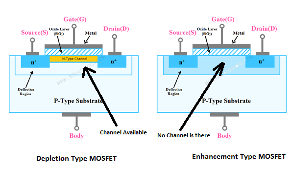
Here you can see the internal construction diagram of both Depletion and Enhancement MOSFET.
You can see in the above diagram, there is a permanent channel in the depletion MOSFET but in the Enhancement MOSFET, there is no Channel. A temporary channel is produced when we apply a voltage across the MOSFET. The gate of the MOSFET is completely insulated by the metal oxide layer of silicon.
MOSFET is a voltage-controlled Device, not Current Controlled. It is the great advantage of a MOSFET that, almost zero current is required to control the load current. MOSFET can be used for both switching and amplifying purposes although it is mostly used for switching purposes only.
In normal conditions, MOSFET does not allow the flow of current through the Drain and Source terminals, but when we apply a voltage to the gate terminal above the threshold voltage it starts to conduct the load current through the Drain and Source Terminals. Like a BJT MOSFET also has a Cut-off Region, a Linear or Ohomic Region, and a Saturation Region. In the cut-off region, MOSFET does not conduct any current. In the linear or ohmic region, load current increases with the increase of gate voltage. In the saturation region, the load current through the MOSFET got stable, it will not increase even in the increase of gate voltage.
MOSFET Uses and Features
1. MOSFET is a semiconductor switching device that is used as an electronic switch.
2. MOSFET is also used in power amplifier circuits. Here, it provides high input impedance and low output impedance.
3. MOSFET is used in small inverter, rectifier circuits. Using the Pulse Width Modulation(PWM) technique desired output is generated.
4. MOSFET used in automatic LED Driver circuits.
5. MOSFETs are used in Motor Driver and motor Controller Circuits.
6. MOSFETs are used in power supply devices such as SMPS(Switched Mode Power Supply) circuits, stabilizer circuits, etc.
Read Also:
- Why Ceramic Capacitors mostly used in Electronic Circuit than others?
- How Proximity Sensor makes our Mobile Phones Smart and Interesting?
- [Actual] Difference between Analog and Digital Signal with Examples
- Why PIV rating is very IMPORTANT when purchasing a Diode?
- Real Ground and Virtual Ground Difference, Use, Example


