Truth Table and applications of all types of Flip Flops-SR, JK, D, T, Master Slave
Truth Table and applications of all types of Flip Flops
Flip Flop is a very important topic in digital electronics. Nowadays the use of semiconductor memory increases. Most of the semiconductor memories are designed by the Flip Flops. Today we are going to know the Truth Table and applications of all types of Flip Flops.There are mainly two types of circuits in digital electronics one is the combinational circuit and another is the sequential circuit.
Flip Flops are very useful elements in making sequential logic circuits.
What is Flip Flop?
Flip Flop is a circuit or device which can store which can store a single bit of binary data in the form of Zero (0) or (1) or we can say low or high.So flip-flops are storage devices.
Types of Flip Flop:
There are various types of flip-flops which are,- SR Flip Flop
- JK Flip Flop
- D Flip Flop
- T Flip Flop
- Master-Slave JK Flip Flop
SR Flip Flop:
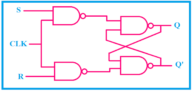
SR flip-flop means Set-Reset flip-flop. It is the basic flip-flop. We can easily set and rest the data bit. When we give the active edge of the clock pulse(that means when the clock pulse is high) then the SR flip-flop changes its contents which means zero to one or one to zero. The SR flip-flop has an indetermined state which is shown in the truth table.The circuit of the SR flip-flop using the NAND gate is Shown below,
 |
| logical circuit diagram of SR flip-flop |
Truth Table of SR Flip Flop:
Input 1 | Input 2 | Initial output condition | Final output condition |
S | R | Q | Q’ |
0 | 0 | 0 | 0 |
0 | 0 | 1 | 1 |
0 | 1 | 0 | 0 |
0 | 1 | 1 | 0 |
1 | 0 | 0 | 1 |
1 | 0 | 1 | 1 |
1 | 1 | 0 | × |
1 | 1 | 1 | × |
Application of SR Flip Flop:
- SR flip-flops are used in control circuits.
JK Flip Flop:
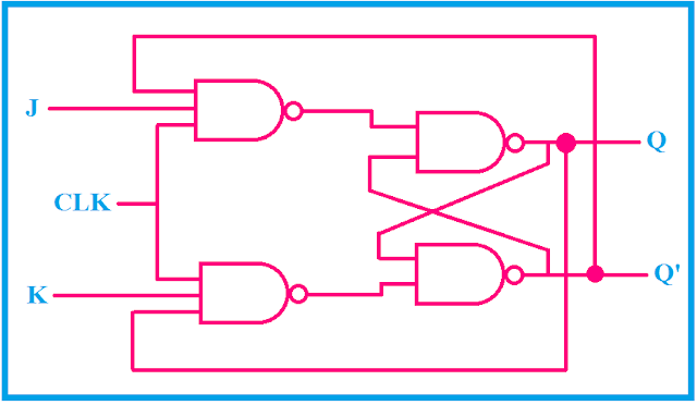
As we know that the SR flip-flop has an indetermined state which is why the JK flip-flops are used. In the JK flip-flop, the S terminal is replaced by the J, and the R is replaced by the K. You can see in the circuit diagram the inputs are connected to the outputs or it takes the output as feedback. For this reason, the JK flip-flop toggles its state when both inputs are asserted.
The circuit of the JK flip-flop circuit using NAND Gate is given below,
Truth Table of JK Flip Flop:
Input 1 | Input 2 | Initial output condition | Final output condition |
J | K | Q | Q’ |
0 | 0 | 0 | 0 |
0 | 0 | 1 | 1 |
0 | 1 | 0 | 0 |
0 | 1 | 1 | 0 |
1 | 0 | 0 | 1 |
1 | 0 | 1 | 1 |
1 | 1 | 0 | 1 |
1 | 1 | 1 | 0 |
Application of JK Flip Flop:
- In frequency division circuit the JK flip-flops are used.
- The JK flip-flops are also used in counters.
D Flip-Flop:
D flip-flop is also called data flip-flop or delay flip-flop. Its construction is also similar to the SR flip-flop except the inputs are connected by NOT Gate. If we see from the outside we will see it has one CLK and one input but actually it has two input. The inputs of the D flip-flop is always opposite as the NOT Gate is connected.
 |
| logical circuit diagram of D flip-flop |
Truth Table of D Flip-Flop:
D | Q | Q’ |
0 | × | 0 |
1 | × | 1 |
Application of D Flip-Flop:
- The D flip-flops are used in counters.
- They also used in shift registers for data transfer application.
T Flip Flop:
T flip-flop is also called toggle flip-flop. the construction of the T flip-flop is same as the JK flip-flop except both input terminal is connected together and taken out one terminal which is known as T terminal or toggle terminal. It also actually two input and one CLK but as the two input terminal is connected together it has one input and one CLK terminal outside.
Truth Table of T Flip Flop:
T | Q | Q’ |
0 | 0 | 0 |
0 | 1 | 1 |
1 | 0 | 1 |
1 | 1 | 0 |
Application of T Flip Flop:
- It acts as a digital toggle switch.
- In frequency divider circuit the T flip-flops are also used.
Master-Slave JK Flip Flop:
The master-slave flip-flop is designed by two JK flip-flops connected in series. The output of the first flip-flop is connected to the input of the second flip-flop. The CLK terminals of the flip-flops are connected through a NOT gate.
When the clock pulse is high the first or master flip-flop is active and when the clock pulse is low the second or slave flip-flop is active.
 |
| logical circuit diagram of a master-slave flip-flop |
The truth table of Master-slave JK Flip-Flop:
Input 1 | Input 2 | Initial output condition | Final output condition | remark |
J | K | Qn+1 | Q’n+1 | |
0 | 0 | Qn | Q’n | Not change |
0 | 1 | 0 | 1 | Reset |
1 | 0 | 1 | 0 | Set |
1 | 1 | Q’n | Qn | Toggle |
Read Also:
Thank you for visiting the website. keep visiting for more updates.


