IC CA3130 and IC CA3140 Pinout Diagram, Features, Datasheet
Here, in this article, we are going to see IC CA3130 and IC CA3140 Pinout Diagram, Pin Configurations, Features, Datasheet, etc. The IC CA3130 and IC CA3140 are operational amplifiers (op-amps) that were commonly used in analog electronic circuits. They were developed by RCA (Radio Corporation of America), now a part of ON Semiconductor. Both the CA3130 and CA3140 have relatively simple internal circuitry and were commonly used in analog signal conditioning, filtering, amplification, and basic analog arithmetic circuits.
IC CA3130 Pinout Diagram
Here, you can see the Pinout Diagram of IC CA3130.
Here are the functions of each pin described below,
Pin 1 and 5 are the Offset Null Pins. These are optionally used to remove the offset voltage at the output pin to make it perfect 0V during off state.
Pin no.2 is the Inverting Input (IN-) Pin. The Inverting pin is also given a fixed voltage which is compared with the (IN+)
Pin no.3 is the Non-Inverting Input (IN+) Pin. The Non-Inverting Pin of the comparator is used to give a variable voltage to compare.
Pin no.4 is the Ground (VCC-) Pin. This pin is to be connected to the ground of the system (Negative voltage can also be used)
Pin no.6 is the Output Pin. This is the output pin of the operational amplifier.
Pin no.7 is the VCC+ Pin. It is used to provide the operating voltage for the Op-Amp. For CA3130 it is up to +16V.
Pin no. 8 is the Strobe Pin. It allows you to turn off the output stage.
IC CA3130 Features
- The CA3130 is a high-input impedance operational amplifier with a single op-amp in the package.
- It is known for its very high input impedance (typically in the order of several megaohms), which makes it suitable for applications requiring a non-invasive input stage.
- It has a rail-to-rail output swing, meaning it can provide an output voltage that comes very close to its supply voltages.
- The CA3130 is known for its low input bias current, which is the amount of current that flows into or out of its input terminals when no external biasing is applied.
- It operates on a single supply voltage and is commonly used in applications such as impedance converters, voltage followers, integrators, and other circuits that require high input impedance.
Download IC CA3130 Datasheet
IC CA3140 Pinout Diagram
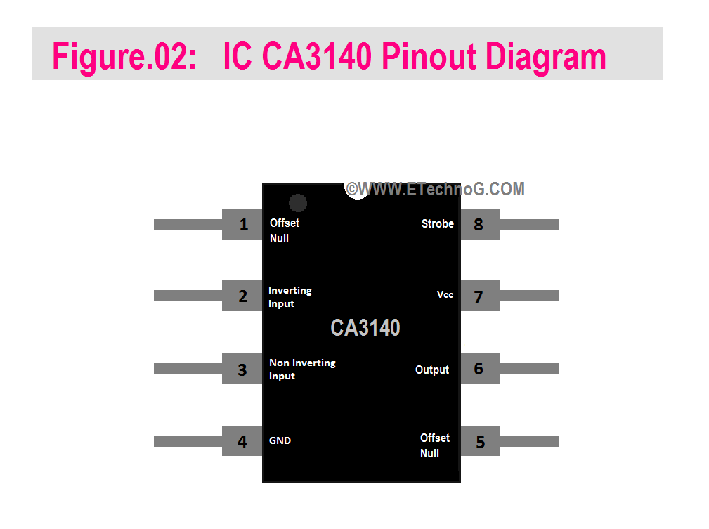
Here, you can see the Pinout Diagram of IC CA3140.
As you can see the Pinout Diagram of IC CA3140 is similar to IC CA3130. So the function of each Pin is also the same that is already described above.
IC CA3140 Features
- The CA3140 is also an operational amplifier with a single op-amp in the package.
- It is an improvement over the CA3130 and offers even higher input impedance and lower input bias current.
- The CA3140 can be used in similar applications as the CA3130, with the advantage of improved performance characteristics.
- Like the CA3130, the CA3140 is also designed to operate on a single supply voltage and provides a rail-to-rail output swing.
Difference between IC CA3130 and IC CA3140
Both the CA3130 and CA3140 are general-purpose op-amps with MOSFET input stages, providing high input impedance and low input bias currents. The main difference is that the CA3140 is characterized as a BiMOS op-amp, which might result in slight variations in performance and characteristics compared to the CA3130. However, for most practical purposes, both op-amps can be used interchangeably in many applications where high input impedance and low input currents are required. It is recommended to always refer to the datasheets for specific details and considerations when designing circuits using these op-amps.
Download IC CA3140 Datasheet
Read Also:


