IC 741 Pinout Diagram and Terminal Identification
In this article, we are going to see the pin diagram of IC 741. IC 741 is an operational amplifier. It is a very popular IC used in so many useful applications. It is primarily designed for analog operations. It can be called as the basic building block of analog electronic circuits. It has so many useful functions. It is also one type of solid-state IC. The operational amplifier IC 741 has a very high voltage gain. It has internal complex circuitry consisting of different types of active and passive elements such as Transistors, resistors, capacitors, and diodes. The IC 741 is mainly used to perform mathematical operations such as addition, subtraction, division, multiplication, differentiation, integration, etc.
It works in three basic stages,
- Differential Input
- Gain
- Push-Pull Output
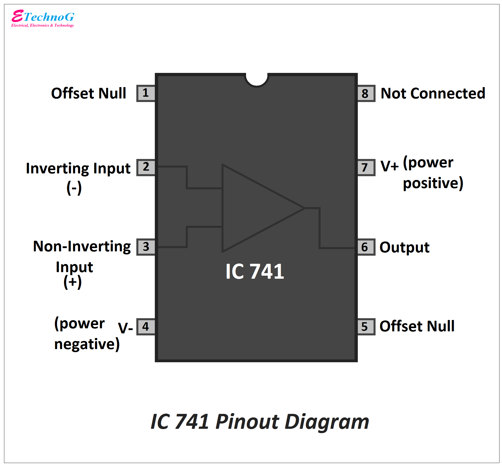
Let's see the IC 741 Pin Diagram.
As you can see it has a total of eight terminals. It comes in an 8-pin DIP(Dual-Inline Package), TO5-8 Metal Can Package, and 8-pin SOIC Package. Here, you can see the pin details for 8 pin DIP Package,
Pin No.1 - Offset Null
Pin No.2 - Inverting Input
Pin No.3 - Non-Inverting Input
Pin No.4 - Negative Power Supply
Pin No.5 - Offset Null
Pin No.6 - Output
Pin No.7 - Positive Power Supply
Pin No.8 - Not Connected
The IC 741 works as a differential amplifier. When we applied the same voltage to the Inverting Input Terminal(Pin 2) and Non-inverting input terminal(pin3), ideally there is no voltage occurs in the output terminal(pin6). Practically, there is some offset voltage that occurs in the output and we should consider it as negligible. When we apply different voltages to the input terminals, the IC will produce a differentiated voltage at its output terminal.
The IC 741 is operated with a 5V to 18V supply voltage. Pin no 7(positive) and pin no 4(negative) are used to provide the power supply.
As we know practically, there is offset voltage occurs in the output when the same voltage applied to its input terminals. So to eliminate or nullify this offset voltage, the offset pins(pin no 1 and 5) are used. By providing an external voltage we can nullify the offset voltage.
Read Also:

