IC TL074 Pinout Diagram and Terminals
IC TL074 is a JFET quad operational amplifier IC. It is a low-noise integrated circuit. In this article, we are going to see the TL074 pinout diagram and its terminal identification. The applications of this IC are single-phase and three-phase uninterruptible power supply(UPS), battery testing devices, audio mixer and audio equalizer circuits, motor driver circuits, etc.
IC TL074 Pinout Diagram
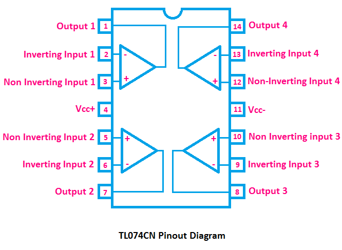
Here you can see the pin diagram of IC TL074.
This IC has a t total of 14 pins.
Pin No. 1 - Output 1
Pin No. 2 - Inverting Input 1
Pin No. 3 - Non-Inverting Input 1
Pin No. 4 - Vcc+
Pin No. 5 - Non-Inverting Input 2
Pin No. 6 - Inverting Input 2
Pin No. 7 - Output 2
Pin No. 8 - Output 3
Pin No. 9 - Inverting Input 3
Pin No. 10 - Non-Inverting Input 3
Pin No. 11 - Vcc-
Pin No. 12 - Non-Inverting Input 4
Pin No. 13 - Inverting Input 4
Pin No. 14 - Output 4
See Also:

