IGBT Symbol, Circuit, Characteristics, Constructional Diagram
IGBT Full Form Insulated Gate Bipolar Transistor. IGBT is a semiconductor switching device. MOSFET and BJT are the most used electronic semiconductor devices. IGBT is designed with the characteristics of both MOSFET and BJT or we can say IGBT is the combination of MOSFET and BJT. IGBT is a three-terminal device and it is capable of carrying a large amount of current and provides a very high switching speed. Although an IGBT can not provide switching speed like a BJT and MOSFET. BJT and MOSFET are low current-carrying devices but provide high switching speeds.
IGBT Symbol
Here you can see the symbol of IGBT below.
You can see IGBT has three terminals named - Gate(G), Emitter(E), and Collector(C). As you can see its symbol shows that it is basically a bipolar junction transistor but its gate is insulated from the main circuit.
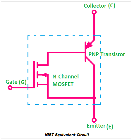
Equivalent Circuit of IGBT
As I already told you before, IGBT is a combination of BJT and MOSFET. In the equivalent circuit, you can see the same.
You can see the Base terminal of the PNP transistor is connected with the collector terminal of the N-Channel MOSFET. The emitter terminals of both BJT and MOSFET are connected together.
Internal Construction of IGBT
Here you can see the internal constructional diagram of IGBT below.
IGBT is a Four Layers(P-N-P-N) device. Body Region, Drift Layer, Injection layer, and Metal layer are shown in the above figure. You can see the metal layer of the gate terminal is insulated from the semiconductors by a Silicon Dioxide(SiO2) metallic layer. There are two emitter terminals connected together. Here you can see two junctions are there. The junction between the P substrate and n-layer is called Junction 2(J2) and the junction between the P layer and n-layer is called Junction 1(J1).
Read Also:
IGBT Characteristics
Here you can see the Switching Characteristics diagram of IGBT.
The X-axis represents the Collector Current(Ic) and the Y-axis represents the Collector-emitter voltage(VCE). From the above diagram, we can see the output characteristic of the IGBT.
When the gate voltage(VGE) is zero, then the device is in the off condition, this is called Cut-off Region.
When the gate voltage increases but below the threshold voltage, there will be a small leakage current but then also the device will be in the cutoff region.
When the gate voltage increases above the threshold voltage, the device will be turned on and go into Active Region. In this active region, the current will flow through the device and the flow of current can be increased by increasing the gate voltage.
When the device goes into the saturation region then the flow of current will be constant it will not increase even increasing the gate voltage.
IGBT Advantages
1. IGBT or Insulated Gate Bipolar Transistor provides very high efficiency.
2. IGBT can work with a very high switching speed.
3. IGBT can handle high current, voltage, and power.
4. As the gate is isolated, so it provides electrical safety during high-voltage operation.
Read Also:


