Pinout Diagram: IC 4000, IC 4001, IC 4002, IC 4006, IC 4007
IC 4000 Pinout Diagram
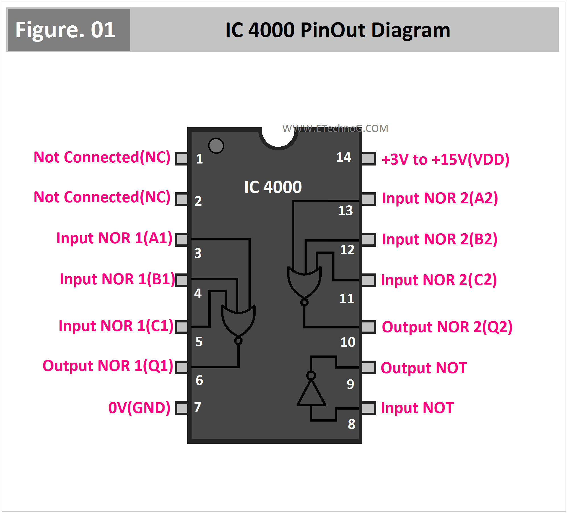
The IC 4000 is a Dual 3-input NOR gate + One inverter gate chip which means it contains two individual NOR gates and a NOT Gate or Inverter in a single integrated circuit. Each NOR gate has three inputs and one output. The NOT gate has one input and one output. Here, you can see the pinout diagram of IC 4000 below, where you can see the names of each pin.
IC 4001 Pinout Diagram
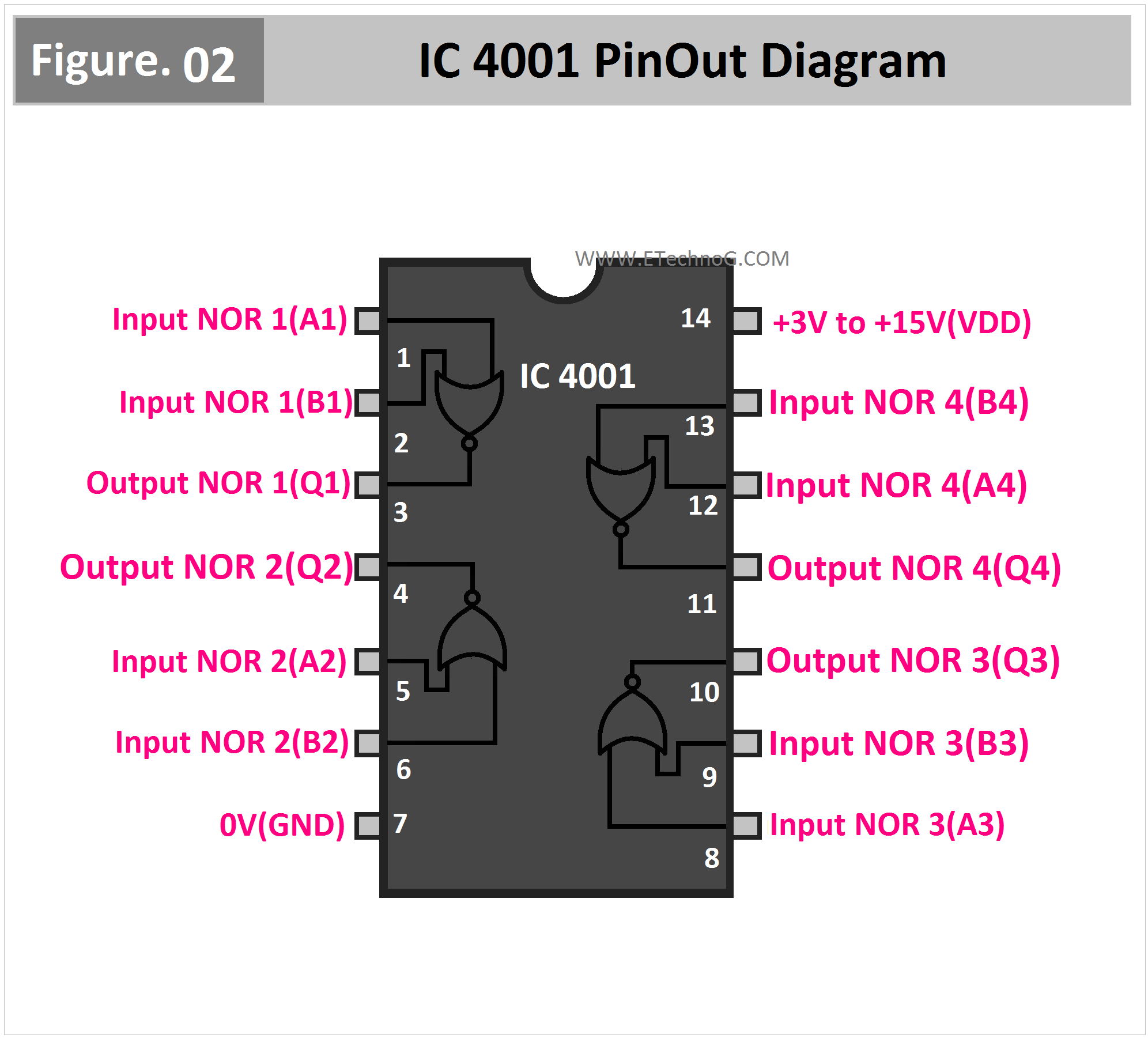
The IC 4001 is a quad 2-input NOR gate chip, which means it contains four individual NOR gates in a single integrated circuit. Each gate has two inputs and one output. Here, you can see the pinout diagram of IC 4001 below.
The gates within the IC 4001 perform logical NOR operations on their inputs. A NOR gate produces an output of 0 (low) only when both of its inputs are 1 (high); otherwise, the output is 1 (high). The IC 4001 is commonly used in digital logic circuitry to perform logical operations and is often integrated into various electronic projects and systems.
IC 4002 Pinout Diagram
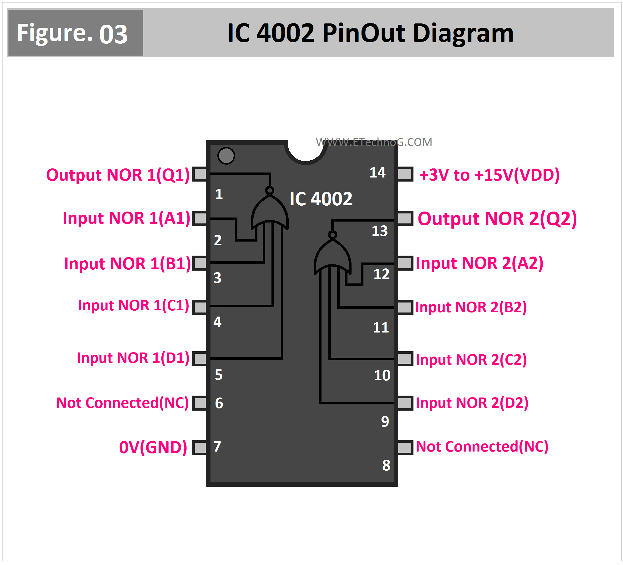
The IC 4002 is a dual 4-input NOR gate chip, which means it contains two individual 4-input NOR gates in a single integrated circuit. Each gate has four inputs and one output. Here, you can see the pinout diagram of IC 4002 below.
IC 4006 Pinout Diagram
The IC 4006 is an 18-stage static shift register and typically comes in a 14-pin package. It has four independent shift registers with a common clock: two 4-stage, two 5-stage with Q4 tap. Here, you can see the pinout diagram of IC 4006 below.
A shift register is a digital circuit that can store and shift binary data sequentially. It's commonly used in applications like serial-to-parallel conversion, data storage, time delay generation, and digital signal processing.
The IC 4006 specifically has 18 stages, which means it can store and shift 18 bits of binary data. Each stage typically consists of a flip-flop (usually D-type) that can hold one bit of data. The clock signal controls when the data is shifted from one stage to the next.
IC 4007 Pinout Diagram
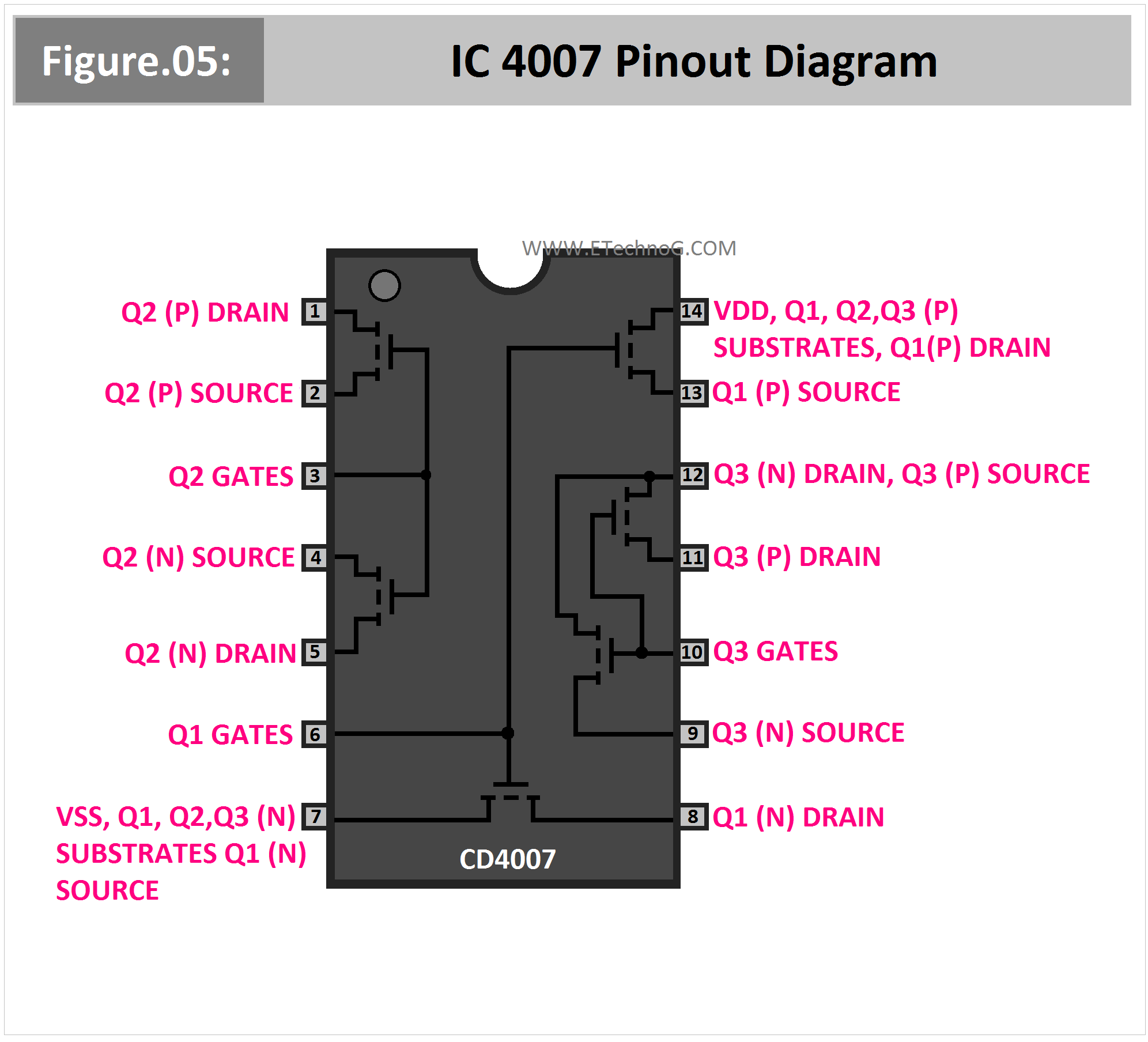
The IC 4007 is a dual complementary enhanced-MOS transistor pair + 1 inverter gate Chip. It has three p-channel and three n-channel enhancement-mode MOSFETs with access to each device. It is commonly used for various analog applications. Here, you can see the pinout diagram of IC 4007 below.
Dual Complementary Pair (Transistor Pair)
The dual complementary pair consists of two sets of complementary MOS transistors. Complementary pairs are used in analog circuitry for tasks like signal amplification, current steering, and switching. The CMOS technology used in this IC allows for low power consumption and high noise immunity.
Inverter Gate
The additional inverter gate in the IC 4007 is a basic digital logic gate that performs inversion. It has one input and one output. When the input is high, the output is low, and vice versa. In digital circuits, inverters are fundamental for signal processing and logical operations.
See Also:


