What is SR Flip Flop? Truth Table, Circuit Diagram Explained
What is SR Flip Flop?
The SR Flip Flop is a bistable device built with a sequential logic circuit that can store a minimum of 1-bit memory data. The SR Flip Flop Stands for Set Reset Flip Flop. It is also known as SR latch. It is the most basic sequential logic circuit. It is built with two logic gates. The output of each gate is connected to the input of the other gate so a feedback signal can go from the output to the input.
The SR flip flop has two inputs named as Set(S) and Reset(R), that is why it is called SR Flip Flop. The rest input is used to get back the flip flop to its old original state from the current state. The output of the flip flop depends upon its inputs such as the input SET(S) making the output 1 while the input RESET(R) making the output 0.
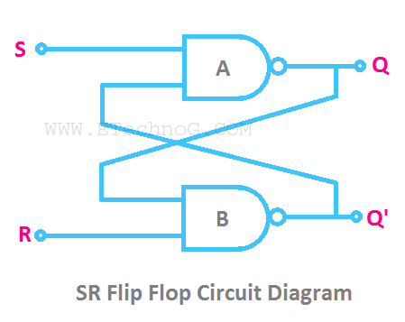
The SR Flip Flop can be built with either NAND gates or NOR gates. A basic SR flip Flop is constructed with NAND gates and it has four terminals - Two Active Low input Terminals(S, R) and two output terminals Q and Q'. This is also called as Flip Flop because during the operation it flipped to a logic set state and flopped back to the opposite logic reset state.
SR Flip Flop Circuit Diagram
Here, you can see a basic SR Flip Flop Circuit using two NAND gates.
Here, you can see the clocked SR Flip Flop Circuit using four NAND gates
SR Flip Flop Truth Table
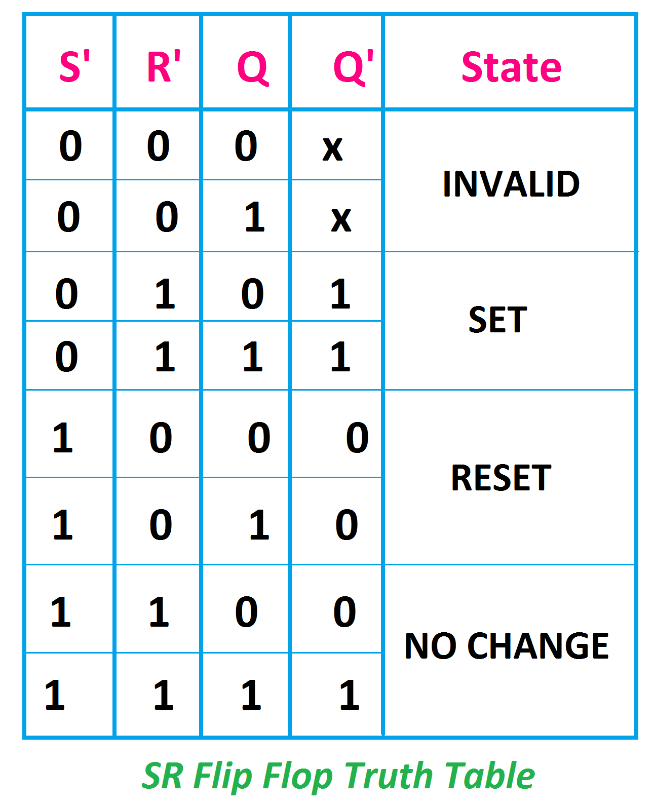
Here, you can see the truth table of SR Flip Flop having two inputs - set and reset
Here, you can see the truth table of SR Flip Flop having three inputs - set, reset, and clock
As you can see in the above truth tables, the two-input SR flip-flop is simple and operates directly on S and R inputs whereas the three-input SR flip-flop has a little bit more complex calculations but it adds flexibility by allowing external control using the Enable input.
SR Flip Flop Operation
You can easily understand the operation of SR Flip Flop by its truth table. You can understand which input provides which output.
The SET State
According to the two NAND gate SR Flip Flop Circuit, when the reset input R is set to low or zero and the set input S is set to high or 1, the NAND gate B will be getting input 0, so the output Q' will be high or 1. As the output of the NAND gate B is connected to the input of the NAND gate A, its both inputs will be high or 1 so the output of the NAND gate A, Q will be low or zero.
Now, when the reset input R is set to high or 1 and the set input S is kept also remain High or 1, the output Q' will be high or 1, and output Q will be low or 0.
The RESET State
When the Set input S is set to low or 0 and the reset is set to high or 1, there will be no change in the state of the flip flop. The flip-flop circuit will be latched. At this time the output Q will be high or 1 and the output Q' will be low or 0.
SR Flip Flop Applications
1. As we know the SR Flip Flop can store 1-bit data. So we can use it in digital memory circuits.
2. SR Flip Flop is used in frequency divider circuits.
3. They are also used in digital counter circuits.
Read Also:


