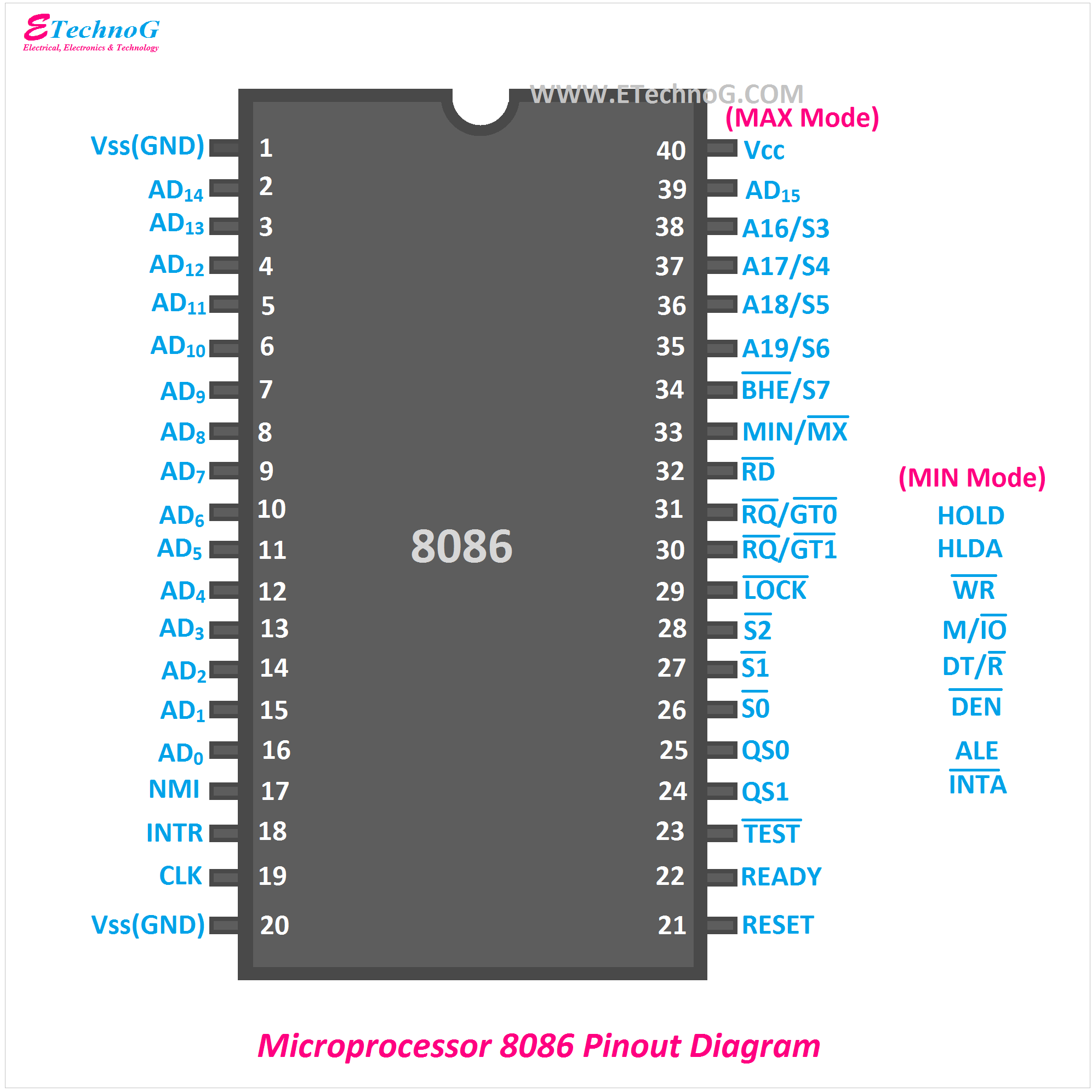
Microprocessor 8086 Pinout Diagram and Pin Description
The microprocessor 8086 is an advanced processor created by Intel in 1978. Like the 8085 microprocessor, 8086 also has 40 pins but it is a 16-bit processor. It is a Dual Inline Package integrated circuit built with HMOS technology. The main specialty of this microprocessor is, it can operate in two different modes - Maximum Mode and Minium Mode. At the minimum mode, the microprocessor works as a single processor while at the maximum mode the microprocessor works as multiple processors. We need to assemble the microprocessor 8086 IC chip in a PCB with its peripheral devices for its practical uses.
Here, you can see the pin diagram of 8086 microprocessor.
Pin No 1
Pin no 1 is the Vss or Ground. It is used to connect with the negative terminal of the power source and ground of the circuit.
Pin No 2 to 16
These are the bidirectional pins. These pins are used to carry both address and data bits. The microprocessor 8086 uses a 20-line address bus. Pins 2 to 16 are named as AD14 to AD0. Here, A indicates the address and D indicates the data. These
Pin No 17
Pin no 17 is the NMI or Non-maskable interrupt. It is used to provide the edge-triggered interrupt signal.
Pin No 18
It is named as INTR. It is also an interrupt pin. It is sampled during the last cycle of the instruction.
Pin No 19
It is used to connect an external crystal oscillator to the microprocessor. During the program or instruction execution, the oscillator provides the pulse or timing signal to the microprocessor. The clock signal is in the form of an asymmetric square wave. The examples of clock frequency are 5MHz, 8MHz, 10MHz.
Pin No 20
Pin no is also the Vss or Ground terminal and is to be connected to the negative terminal of the power source.
Pin No 21
Pin no 21 is the RESET. It is used to reset the microprocessor or terminate its all current program executions. The signal is to be high for the first 4 clock cycles to reset the microprocessor and all the devices connected to it.
Pin No 22
Pin no 22 is READY. It is used to communicate between the microprocessor and external devices so that they can notify that they are ready to communicate or ready to send or receive signals. It works with the active high signal. That means when the signal is high, it indicates that the devices are ready. If the signal is low, it indicates that the devices are not ready, so wait for it.
Pin No 23
Using this 'Wait' instruction is to be provided. When the signal in this pin is low the program execution in the microprocessor remains continuing but if the signal in this pin is high it pauses the operation.
Pin No 24 and 25
In the maximum mode of the microprocessor, QS1 and QS0 are used for the queue status signals such as whether 'there is no operation', 'first-byte opcode', 'empty queue', and 'subsequent byte from the queue'. In the minimum mode, these are works as INTA(Interrupt acknowledge) and ALE(Address Latch Enable)
Pin No 26 to 28
Maximum Mode - S0, S1, and S2 are the status pins. During the read, write operations with memory or any communication with I/O devices, these pins show the status such as 'interrupt acknowledgment', 'I/O read and write operations', 'Memory Read and Write operations', 'Halt', 'Code Acess', etc.
Minimum Mode - 26, 27, and 28 are work as DEN', DT/R', and IO'/M respectively.
Pin No 29
In the maximum mode, it acts as a Lock'. It is used to lock the bus while a program executes so other systems cannot use the system bus.
In the minimum mode, it acts as a Write(WR') pin that is used to store data to the external memory.
Pin No 30 and 31
In the maximum mode, they act as RQ'/GT1' and RQ'/GT0'. The RQ/GT means request/grant. These are the bi-directional pins and they are used to request the processor to leave the system bus.
In the minimum mode, they act as HOLD and HLDA(hold acknowledge) respectively.
Pin No 32
It is the Read(RD') pin. It is an active low pin and is used to fetch data from the external memory to the microprocessor.
Pin No 33
Using this pin the operating mode of the microprocessor can be changed. When the signal in this pin is low, the microprocessor will operate in maximum mode, and when the signal in this pin is high, the microprocessor will operate in minimum mode.
Pin No 34
Pin no 34 is BHE'/S7. That means Bus High Enable/ Status. Bus High Enable is the active low and status is the active high.
Pin No 35 to 38
Pins from 35 to 38 are used for the carrying of addresses and data bytes. Also, they use it for status.
Pin no 39
It is used to carry addresses and data bytes.
Pin No 40
Pin no 40 is the Vcc and it is used to connect the positive terminal of the power supply.
Read Also:

