Rectifier Circuit Diagram | Half Wave, Full Wave, Bridge
In this article, we are going to see all types of rectifier circuit diagrams such as Circuit Diagram of Half Wave Rectifier, Circuit Diagram of Full Wave Rectifier, and Circuit Diagram of Bridge Rectifier.
The rectifier is an electrical or electronic circuit that converts alternating current into direct current. Generally, a simple rectifier circuit is made up using PN Junction Diodes. Those PN Junction Diodes allow the flow of current in one direction only.
The main function of a rectifier circuit is to take the AC supply as input and to provide DC supply as output. Also, note that a rectifier circuit cannot provide a pure DC in its output. There AC components always present in the output DC and known as Ripple. So, a filter circuit made by a capacitor or inductor is always connected to the output of the rectifier circuit to remove the ripple.
Half Wave Rectifier Circuit Diagram
Here, you can see the circuit diagram and input-output waveform of the Half Wave Rectifier.
Here, you can see the half-wave rectifier circuit is consisting a single PN Junction Diode. This allows the current for only one half cycle of the AC that is the positive half cycle. During the negative half cycle, the PN Junction Diode will block the current. So, in the output, the current will flow in one direction only like the DC power supply.
Here, you can see three waveforms are there. The first one is for the input AC supply or transformer primary side. The second one is for the transformer secondary side. As the transformer steps down the voltage, the magnitude of the waveform is also reduced. The third one is for the output of the rectifier circuit. In this waveform, you can see only positive half cycles are shown. Also, remember that the transformer is not a part of the rectifier circuit. If there is no transformer then also it will convert the AC into DC.
You can see the example of half wave rectifier circuit in soldering iron, where a single Diode is connected in series. Here, the diode not only used for the rectification, it also used to reduce average voltage.
The main disadvantage of the half wave rectifier is that it reduces the voltage in its output voltage from the actual input voltage. This happens because the diode allows positive half cycles only. So the average output voltage will be half of the main input voltage.
Simple circuit design, low cost, etc are the advantages of a half wave rectifier.
Read Also:
Centre Tap Full Wave Rectifier Circuit Diagram
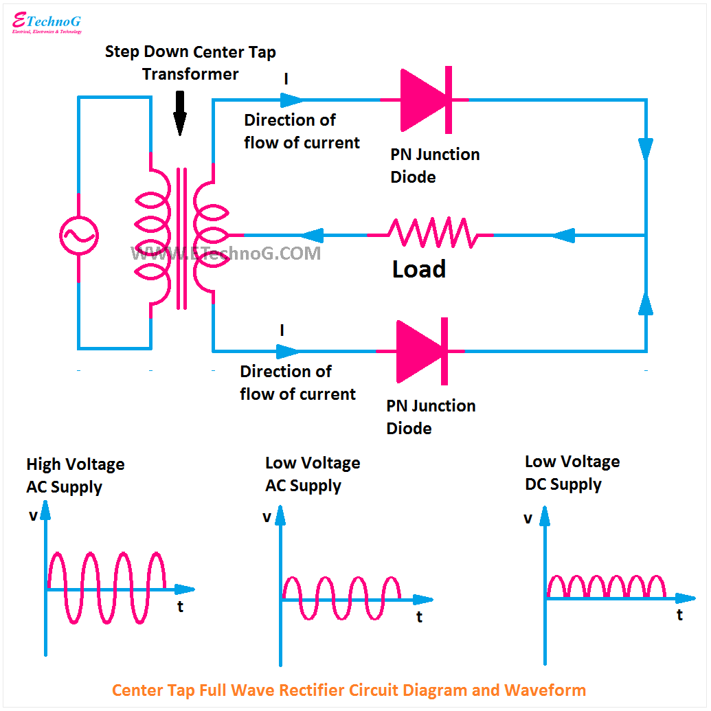
Here you can see the circuit diagram and input-output waveform of Full Wave Rectifier with a Centre Tapped Transformer.
Here, you can see, two PN Junction Diodes are used to make this rectifier circuit. The upper one only allows the positive half cycles and the lower one allows the negative half cycles. The diodes are connected to the load in such a way that the current can flow in one direction only through the load. So, the load will experience the DC voltage and DC current. This centre tapped step-down transformer is designed in such a way that the upper part and the lower part of the secondary winding produce the same voltage.
Here also, you can see three waveforms are there. The first one is for input AC power supply to the transformer. The second one is for transformer secondary or output. The third one is for the rectifier output. Here you can see there is no gap between the positive half cycles like half wave rectifier waveform. Here, negative cycles are also converted into positive cycles. So, the waveform is continuous.
This full wave rectifier circuit also cannot provide pure DC. Here also ripples available. We can remove these ripples by using an filter circuit at the output of the rectifier circuit. The main advantage of this full wave rectifier circuit is it does not lower or reduce the output voltage from the input voltage like a half wave rectifier circuit. Here also a disadvantage available that is, it requires a centre tapped transformer. So, designing coat increases.
Read Also:
Full Wave Bridge Rectifier Circuit Diagram
Here you can see, the circuit diagram and input-output waveform of the bridge rectifier.
Here, you can see a total of four PN Junction Diodes are used to make this rectifier circuit. Four diodes are connected in such a way that a bridge like structure is formed, and it has four sides to connect input and output terminals.
Here also, three waveforms are there. The first one is for transformer input or primary side, the second one is for transformer secondary or output side. And the third one is for rectifier output. The output waveform of both the centre tap and bridge rectifier is the same.
The full wave bridge rectifier circuit has so many advantages over others. Bridge rectifier has high efficiency than others. It does not require any centre tapped transformer. So, the designing cost also very low.
Read Also:


