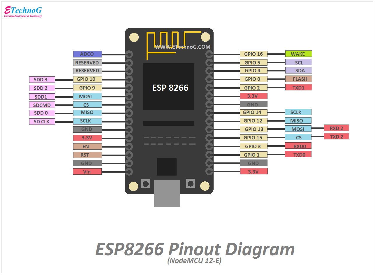
ESP 8266 Pinout Diagram | 12E NodeMCU
In this article, we are going to see the pinout diagram of ESP 8266, 12E NodeMCU. ESP 8266 is a microchip used for high-quality Wifi Network solutions for electronics circuits, devices projects, etc. Nowadays, it is the most important and widely usable device in the sector of the Internet of Things(IoT) industry. It is the best device among the other internet devices. The main features of this device are low cost, high performance, low power consumption, compact design, etc. There are different versions of ESP8266 such as the 12E module, 12E Wemos D1 Mini output, 01 Module, and 12E NodeMCU.
The ESP 8266 can work as a slave with a microcontroller to provide the internet or local networking access through Wifi technology. Also, it can be used for standalone applications. It can be interfaced with the microcontroller with SPI or UART protocols. It is built with a 32-bit processor, on-chip SRAM, RF Receiver, RF Transmitter, Analog Transmitter, Analog Receiver, Digital baseband, Amplifiers, filters, and other components.
Let's See the ESP8266 Pin Diagram
The ESP 8266, 12 E Node MCU has a total of 30 pins. Among these 14 pins are active. It also has an onboard flash or reset button, 3.3V voltage regulator, Micro USB, etc.
It has around 17 GPIO pins but only 13 are brought out to outside for the external connection. Other pins are connected internally for the processor and other peripheral interfacings. Also, you can see this board has a total of 8 power supply pins among which 3 nos 3.3V power out pins, 3 nos grounding pins, and 1 no 5V Vin or Power In pin. The GPI0 is connected to the flash button. So it can be flashed or reset by the flash button or by the external signal through the GPI0 Pin.
See Also:

